

A revolution in the world of microchips: TSMC has announced the construction of two fabs for the production of state-of-the-art 2-nm chips
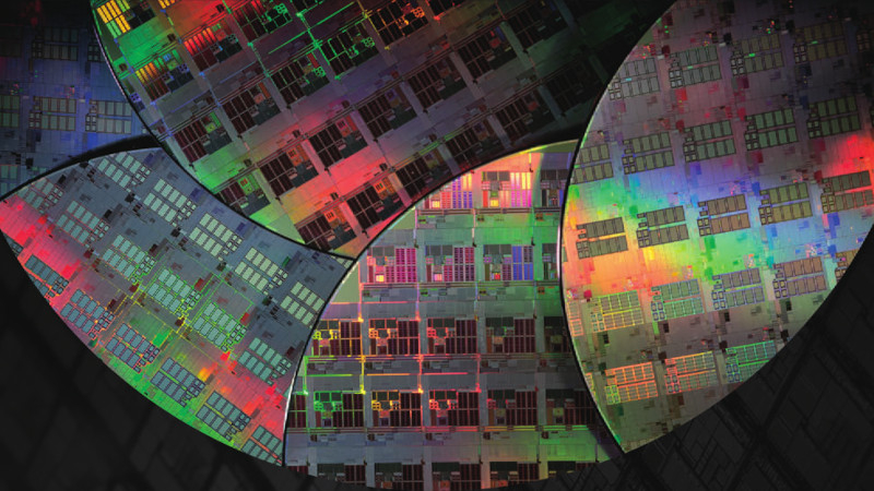
Taiwan Semiconductor Manufacturing Co. (TSMC), a leading global semiconductor manufacturer, has announced the start of construction of two new fabs to design and manufacture chips based on the advanced 2-nanometer (N2) process. Additionally, preparatory work is underway for the construction of a third factory, which is to begin after receiving approval from the Taiwanese government.
Mark Liu, Chairman of the Board of Directors of TSMC, shared the company’s plans during a conversation with analysts and investors, expressing confidence in the start of mass production of chips using the 2-nm process in 2025. He also mentioned the company’s commitment to deploying multiple production sites in Hsinchu and Kaohsiung Science Parks to meet growing demand.
The first fab will be located near Baoshan in Hsinchu, close to the R1 research center, which was specifically created to develop 2-nm technology. The fab is expected to start mass production of 2-nm semiconductors in the second half of 2025. The second fab, also designed to produce 2-nm chips, will be located in Kaohsiung Science Park, part of Taiwan’s Southern Science Park. Its launch is scheduled for 2026.
Additionally, TSMC is actively working on obtaining permits from the Taiwanese authorities to build another fab in Taichung Science Park. If the construction of this facility starts in 2025, it will be able to start operating in 2027. With the commissioning of all three fabs capable of producing chips using the 2-nm process, TSMC will significantly strengthen its position in the global semiconductor market by offering customers new facilities for the production of next-generation chips.
The company’s plans for the near future include the start of mass production using the 2-nm process, which includes the use of transistors with nanosheets and circular gates (GAA) in the second half of 2025. By 2026, an improved version of this process is expected to be introduced, which is expected to provide power from the back of the crystal, thus expanding the possibilities of mass production.