


Samsung will launch mass production of 3GAE process chips this quarter using GAAFET transistors (MBCFET)
Samsung has said it is preparing for large-scale production of chips based on the 3GAE (3 nm-class gate all-around early) production process this quarter. This will be the industry’s first 3nm class technology, as well as the first node to use GAAFET (gate-all-around field effect transistors).
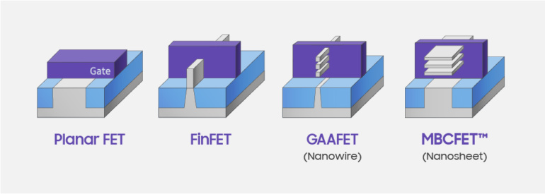
For reference: the GAAFET architecture, which replaces the current FinFET, has been developed by an organization that includes IBM, Globalfoundries and Samsung since 2000. It should help to overcome the physical limitations of the ILO’s scaling. The main feature of GAAFET – ring gates (hence the name gate-all-around FET). The channels of GAAFET transistors are nanowires (they are formed of several horizontal silicon ‘nanosheets’). At the same time, the FinFET channel of the transistor under the gate is a monolithic vertical structure ‘fin’, which imposes restrictions on scaling.
Samsung has its own implementation of GAAFET technology, which has the marketing name Multi-Bridge-Channel FET (MBCFET). In fact, MBCFET differs from GAAFET not only in name but also technically: in the case of Samsung, the channels are made in the form of flat bridges, not wires.
Samsung Foundry’s 3GAE process is the company’s first process to use GAA transistors called MBCFETs. Earlier, Samsung said that this process will increase performance by 30%, reduce power consumption by 50% and increase the density of transistors to 80% (including a combination of logic transistors and SRAM transistors).
Theoretically, GAAFET technology has a number of advantages over the FinFET currently in use. In GAA transistors, the channels are located horizontally and surrounded by gates. The channels are formed using epitaxy and selective removal of materials, which allows you to fine-tune them by adjusting the width of the transistor channel. High productivity is achieved due to wider channels, low energy consumption – due to narrower channels. This accuracy significantly reduces the leakage current of the transistor (ie reduces power consumption), as well as the variability of the performance of the transistor, which provides faster time to market and the possibility of higher income. In addition, GAAFET will reduce the cell area by 20-30%.
The Samsung 3GAE process, as an ‘early’ 3-nm production technology, will be used mainly by Samsung LSI and possibly one or two other large Samsung Foundry customers. Given that such customers and Samsung LSI tend to produce chips in very large quantities, it can be expected that 3GAE technology will be widely used, provided that the performance and efficiency of these products meet expectations.